| FRESCOES ROOM | |||||
|
WS.VIII EXPLORING STRESS AND STRAIN IN THIN FILMS AND SEMICONDUCTOR MATERIALS September 12 |
|||||
| Co-organized with: | |||||
 |
 |
||||
|
WORKSHOP COMMITTEE |
|||||
|
This workshop provides a focused platform for researchers and professionals to discuss the latest developments and research results related to stress and strain in thin films and semiconductor materials. Co-organised by Roma Tre University and Sapienza University of Rome, the event is structured into two distinct sessions, each dedicated to a specific aspect of the topic. The first session will focus on stress in thin films, covering topics such as the origin and control of residual stress, advanced measurement techniques and the impact of stress on the reliability of micro-electro-mechanical systems (MEMS). The second session will focus on strain in semiconductor materials, discussing the effects of strain on material properties, recent advances in measurement and control techniques, and the challenges of managing strain for improved material performance. This split allows for an in-depth exploration of both stress and strain, providing participants with a comprehensive understanding of the interrelationships and differences between these two critical areas of materials science. The workshop brings together leading experts in the field to share their insights and latest research, providing valuable opportunities for learning and collaboration. |
|||||
| September 12 | ||||||||
| 09:00 - 10:30 Stress in Thin Films WS.VIII.1 - TT.V.C |
||||||||
| Chair: Marco SEBASTIANI, Roma Tre University | ||||||||
| This session is the first part (of two) of the workshop on 'Exploring Stress and Strain in Thin Films and Semiconductor Materials' with the aim to provide a focused platform for researchers and professionals to discuss the latest developments and research results related to stress and strain in thin films and semiconductor materials. Co-organised by Roma Tre University and Sapienza University of Rome, the event is structured into two distinct sessions, each dedicated to a specific aspect of the topic. This first session will focus on stress in thin films, covering topics such as the origin and control of residual stress, advanced measurement techniques and the impact of stress on the reliability of micro-electro-mechanical systems (MEMS). The second session will focus on strain in semiconductor materials, discussing the effects of strain on material properties, recent advances in measurement and control techniques, and the challenges of managing strain for improved material performance. This split will allow for an in-depth exploration of both stress and strain, providing participants with a comprehensive understanding of the interrelationships and differences between these two critical areas of materials science. The workshop brings together leading experts in the field to share their insights and latest research, providing valuable opportunities for learning and collaboration. | ||||||||
| WS.VIII.1.1 TT.V.C.1 |
Rostislav DANIEL Montanuniversität Leoben, Austria Origins and control of residual stress in thin films |
 |
||||||
| WS.VIII.1.2 TT.V.C.2 |
Edoardo ROSSI Roma Tre University High resolution measurement Techniques for Stress in Thin Films |
 |
||||||
| WS.VIII.1.3 TT.V.C.3 |
Savvas ORFANIDIS National Technical University of Athens, Greece NanoMECommons: Harmonisation of EU-wide nanomechanics protocols and relevant data exchange procedures, across representative cases; standardisation, interoperability, data workflow |
 |
||||||
| WS.VIII.1.4 TT.V.C.4 |
Matthieu LE BAILLIF Thales Researche and Technology, France Residual Stress and reliability in Micro-Electromechanical Systems (MEMS) |
 |
||||||
| WS.VIII.1.5 TT.V.C.5 |
Saqib RASHID Roma Tre University In-situ measurement of residual stress in MEMS devices |
 |
||||||
| 11:30 - 13:00 Strain in Semiconductor Materials 1/2 WS.VIII.2 - TT.VI.C |
||||||||
| Chair: Stefano LUPI, Sapienza University of Rome (to be confirmed) | ||||||||
| This session is the second part (of two) of the workshop on 'Exploring Stress and Strain in Thin Films and Semiconductor Materials' with the aim to provide a focused platform for researchers and professionals to discuss the latest developments and research results related to stress and strain in thin films and semiconductor materials. Co-organised by Roma Tre University and Sapienza University of Rome, the event is structured into two distinct sessions, each dedicated to a specific aspect of the topic. This session will focus on strain in semiconductor materials, discussing the effects of strain on material properties, recent advances in measurement and control techniques, and the challenges of managing strain for improved material performance. The other and previous session will focus on stress in thin films, covering topics such as the origin and control of residual stress, advanced measurement techniques and the impact of stress on the reliability of micro-electro-mechanical systems (MEMS). This split will allow for an in-depth exploration of both stress and strain, providing participants with a comprehensive understanding of the interrelationships and differences between these two critical areas of materials science. The workshop brings together leading experts in the field to share their insights and latest research, providing valuable opportunities for learning and collaboration. | ||||||||
| WS.VIII.2.1 TT.VI.C.1 |
Lorenzo MONACELLI - CV Sapienza University of Rome, Italy The origin of out-of-equilibrium ferroelectricity in SrTiO3 under resonant ultrafast THz pumping |
 |
||||||
| WS.VIII.2.2 TT.VI.C.2 |
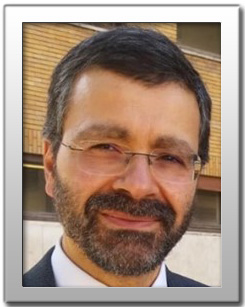
Antonio POLIMENI - CV Sapienza University of Rome, Italy Giant enhancement of light emission from InSe in selectively strained InSe/MS2 (M=Mo,W) heterostructures |
 |
||||||
| WS.VIII.2.3 TT.VI.C.3 |
Elena STELLINO - CV Sapienza University of Rome, Italy Tuning the Excitonic Response of Monolayer WS2 Domes via Coupled Pressure and Strain Variation |
 |
||||||
| WS.VIII.2.4 TT.VI.C.4 |
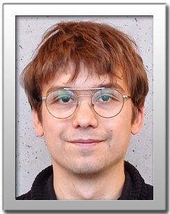
Pablo HERNANDEZ LOPEZ - CV Humboldt Universitat zu Berlin, Germany Strain tuning of optical properties in 2D semiconductors and optical readout of strain in thin films |
 |
||||||
| 14:00 - 15:30 Strain in Semiconductor Materials 2/2 WS.VIII.3 - TT.VII.C |
||||||||
Organized and under the coordination of H2020 Project CHALLENGES |
||||||||
| Chair: Marco VITTORI ANTISARI, Sapienza University of Rome | ||||||||
| WS.VIII.3.1 TT.VII.C.1 |
Chiara MANCINI - CV Sapienza University of Rome, Italy Strain analysis in semiconductor devices through Tip-Enhanced Raman Spectroscopy |
 |
||||||
| WS.VIII.3.2 TT.VII.C.2 |
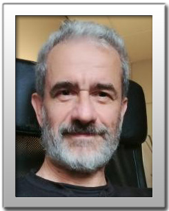
Roberto BALBONI - CV IMM-CNR Measuring crystals strain in the TEM: techniques and accuracy |
 |
||||||
| WS.VIII.3.3 TT.VII.C.3 |
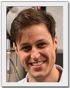
Frederik OTTO - CV Technische Universität Berlin Analyzing Dynamic Diffraction at Strained Semiconductor Interfaces: A Method to Determine Alloy Concentrations |
 |
||||||
| WS.VIII.3.4 TT.VII.C.4 |
Stefan WUNDRACK - CV Physikalisch-Technische Bundesanstalt, Germany Metrological Raman shift calibration for strain quantification in semiconductor |
 |
||||||
| WS.VIII.3.5 TT.VII.C.5 |
Stefano LUPI Sapienza University of Rome, Italy Optoelectronic Properties of Topological Quantum Materials |
 |
||||||
| Back to Overview | Go to Plan 12 September | ||


