| FRESCOES ROOM | |||||
|
WS.VII WIDE-BANDGAP SEMICONDUCTORS AND HETEROSTRUCTURES FOR POWER AND RF ELECTRONICS September 11 |
|||||
| Co-organized with: | |||||
 |
 |
||||
|
WORKSHOP COMMITTEE |
|||||
|
Due to their outstanding physical properties, wide-bandgap (WBG) semiconductors, such as silicon carbide (SiC) and gallium nitride (GaN), are the materials of choice for high-power and high frequency electronics, with a broad range of applications in strategic fields, like electric vehicles, power conversion for renewable energies, aerospace, telecommunications. |
|||||
| September 11 | ||||||||
| 11:30 - 13:00 Wide-bandgap semiconductors and heterostructures for power and RF electronics 1/3 WS.VII.1 - TT.II.B |
||||||||
| Chair: Filippo GIANNAZZO, IMM-CNR - Co-organized with IMM-CNR & iENTRANCE@ENL | ||||||||
| This session will provide an overview on recent development of SiC, GaN and Ga2O3 materials and technology. | ||||||||
| WS.VII.1.1 TT.II.B.1 |
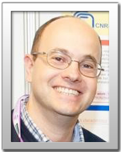
Fabrizio ROCCAFORTE - CV CNR-IMM, Catania Advanced processing for energy efficient WBG semiconductors power devices: Recent trends and perspectives |
 |
||||||
| WS.VII.1.2 TT.II.B.2 |
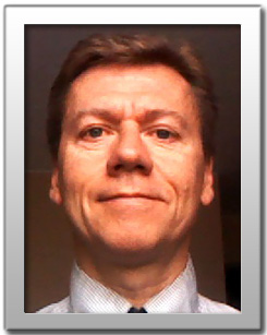
Yvon CORDIER - CV Université Côte d’Azur, CNRS-CRHEA, Valbonne, France Recent advances in Nitride heterostructures for RF and power devices |
 |
||||||
| WS.VII.1.3 TT.II.B.3 |
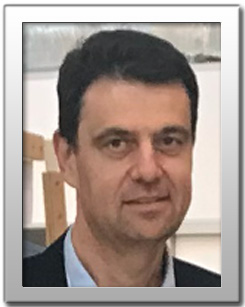
Daniel ALQUIER - CV University of Tours, France Laser Annealing A New Strategy For SiC Power Device Contacts |
 |
||||||
| WS.VII.1.4 TT.II.B.4 |
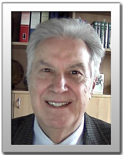
Roberto FORNARI - CV University of Parma Development and perspectives of Ga2O3 epitaxial layers for power electronics |
 |
||||||
| 14:00 - 15:30 Wide-bandgap semiconductors and heterostructures for power and RF electronics 2/3 WS.VII.2 - TT.III.B |
||||||||
| Chair: Luca SERAVALLI, CNR-IMEM - Co-organized with IMM-CNR & iENTRANCE@ENL | ||||||||
| This session will be focused on advanced physical and electrical characterization methods for (U)WBG materials and devices. | ||||||||
| WS.VII.2.1 TT.III.B.1 |
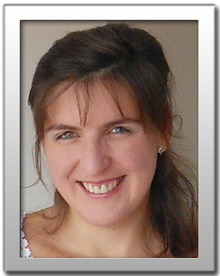
Ildiko CORA - CV HUN-REN, Institute for Technical Physics and Materials Science, Hungary Advanced structural characterization of Gallium Oxide by electron microscopy |
 |
||||||
| WS.VII.2.2 TT.III.B.2 |
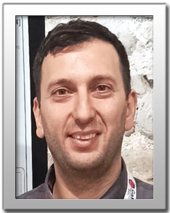
Giuseppe GRECO - CV CNR-IMM, Catania Recent findings on Ohmic and Schottky contacts to β-Ga2O3 |
 |
||||||
| WS.VII.2.3 TT.III.B.3 |
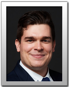
Manuel FREGOLENT - CV University of Padova Trapping processes in vertical GaN Trench MOSFETs: from experimental analysis to simulations |
 |
||||||
| WS.VII.2.4 TT.III.B.4 |
Béla PÉCZ - CV HUN-REN, Institute of Technical Physics and Materials Science, Hungary Advanced electron microscopy of WBG semiconductors and their heterostructures with 2D materials |
 |
||||||
| 16:00 - 17:30 Wide-bandgap semiconductors and heterostructures for power and RF electronics 3/3 WS.VII.3 - TT.IV.B |
||||||||
| Chair: Patrick FIORENZA, IMM-CNR & iENTRANCE@ENL | ||||||||
| This session will present recent developments in the integration of 2D materials (graphene, MoS2) with Nitride semiconductors. | ||||||||
| WS.VII.3.1 TT.IV.B.1 |
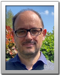
Luca SERAVALLI - CV CNR-IMEM, Parma Recent advances in the liquid precursors chemical vapor deposition (CVD) of MoS2 on SiO2 and on GaN |
 |
||||||
| WS.VII.3.1 TT.IV.B.1 |
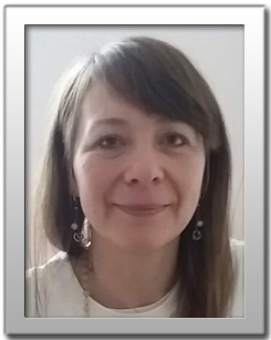
Federica BONDINO - CV CNR-IOM, Trieste Advanced soft-x absorption and photoemission spectroscopy of 2D materials and their heterostructures |
 |
||||||
| WS.VII.3.1 TT.IV.B.1 |
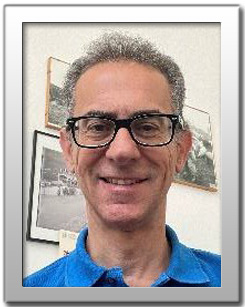
Simonpietro AGNELLO - CV University of Palermo Thermally induced strain and doping of monolayer MoS2 on metal, insulator and WBG substrates |
 |
||||||
| WS.VII.3.1 TT.IV.B.1 |
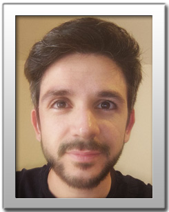
Salvatore Ethan PANASCI - CV CNR-IMM, Catania Integration strategies and nanoscale electrical characterization of MoS2 on WBG semiconductors |
 |
||||||
| Back to Overview | Go to Plan 11 September | ||


